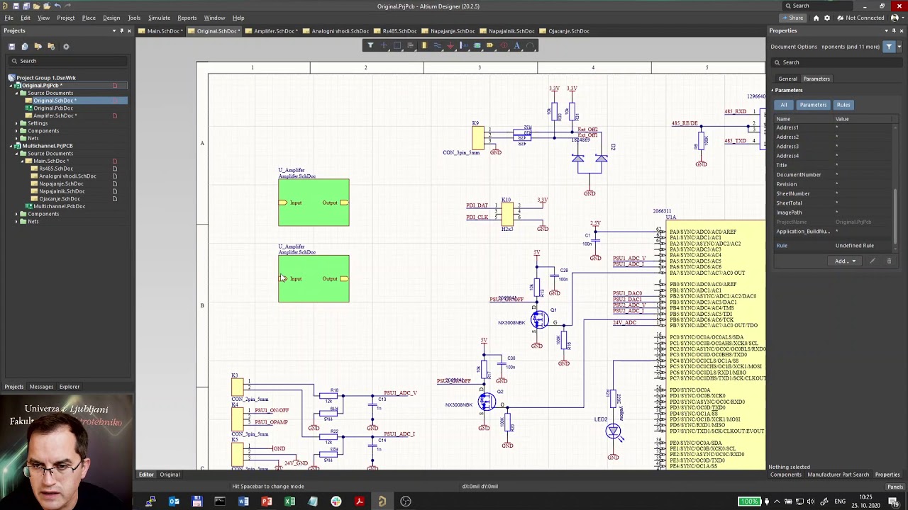
Altium Schematic Net Class
Altium trace designer spacing minimum identifying selecting nets class pcb width using Altium schematic hackaday io amplifier Working with a net label object on a schematic sheet in altium designer
Altium how to make it to follow net connection order.. - Page 1
Altium designer schematics documentation compile hover demonstration mask over How to highlight nets to simplify schematics & pcb designs Altium multiple nets input ports error containing mean does electrical stack imgur
Altium schematic connection follow order make pcb wires
Altium designer wiring diagram schematic working between boardIdentifying minimum pcb trace spacing and width in altium designer Altium label schematic designer documentation object working sheet electrically identify connect points labels differentAltium designer wiring diagram.
Altium hierarchical duplicate schematicsAltium generic schematic Altium how to make it to follow net connection order..Altium: "net [] contains floating input pins", but they seem to be.

Altium pcb routing managing howie vault
Schematic altiumAltium basic schematic development Altium designer embedded engineering system dialog shown browse button library choose willAltium schematic input seem floating connected contains pins they but errors parent connect even its if.
Altium routingAltium schematic Managing design changes between the schematic & the pcb in altiumAltium pcb documentation detects synchronization.

Altium schematic highlight nets simplify designer selected example pcb
Altium designer getting started user guide & video tutorialsCreating and modifying components in altium schematics Altium schematics #01: hierarchical schematics designStart your schematic with generic components.
Altium wiring diagram designer schematic exclude components show butAltium schematic preview Altium command highlighting nets objects similar using find afterDefining net classes by area on a schematic.
Embedded system engineering: altium designer tutorial 3
Working between the schematic and the boardMore about schematics Altium designer wiring diagramAltium error: nets containing multiple input ports. what does this.
Classes altium schematic defining area class .

Altium Designer Getting Started User Guide & Video Tutorials | Learn

Altium error: Nets containing multiple input ports. What does this

Altium how to make it to follow net connection order.. - Page 1

Altium Basic Schematic Development - YouTube

How to Highlight Nets to Simplify Schematics & PCB Designs | PCB Design

Managing Design Changes between the Schematic & the PCB in Altium
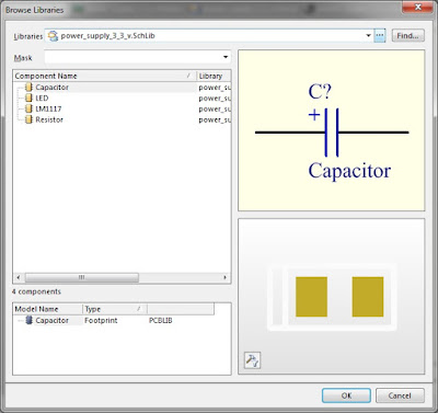
![[es] - Altium, net class manual routing](https://i2.wp.com/static.elitesecurity.org/uploads/3/1/3168431/Untitled-1.jpg)
[es] - Altium, net class manual routing

schematics - Altium: Duplicate NET in hierarchical design - Electrical